UAC 3553B
Universal Serial Bus
(USB) DAC
Edition May 21, 2003
6251-595-1DS
DATA SHEET
MICRONAS
MICRONAS

UAC 3553B
DATA SHEET
2
May 21, 2003; 6251-595-1DS
Micronas
Contents
Page
Section
Title
4
1.
Introduction
4
1.1.
Features
6
2.
Hardware Description
7
2.1.
General Information
7
2.2.
Universal Serial Bus (USB)
7
2.2.1.
Transceiver
7
2.2.2.
USB-Interface
7
2.2.3.
Microcontroller
7
2.3.
GPIO
7
2.4.
General Purpose Timer
8
2.5.
Audio Streaming Interface
8
2.6.
Audio Control Interface
8
2.7.
The I
2
S - Interface
8
2.7.1.
Asynchronous I
2
S input
8
2.7.2.
Synchronous I
2
S Input Mode
9
2.8.
Power Supply
9
2.9.
I
2
C Bus Interface
9
2.9.1.
I
2
C Master
9
2.9.2.
I
2
C Slave
10
2.10.
Analog Output
10
2.10.1.
Digital-to-Analog Converters
10
2.10.2.
Analog Filter
10
2.10.3.
Analog Volume
10
2.10.4.
Line-out/Headphone Amplifier
11
2.11.
Special I/O
11
2.11.1.
SOF (Start of Frame)
11
2.11.2.
SEN (Suspend Enable)
11
2.11.3.
Suspend
11
2.11.4.
Reset
11
2.12.
Clock System
12
3.
Audio Processing
13
3.1.
Automatic Gain Control
13
3.2.
Quasi-Peak
13
3.3.
Bass Control
13
3.4.
Treble Control
14
3.5.
Parametric Equalizer
14
3.6.
Volume, Mute, and Balance Control
14
3.7.
Micronas Dynamic Bass (MDB)
15
3.7.1.
Dynamic Amplification
15
3.7.2.
Adding Harmonics

Contents, continued
Page
Section
Title
DATA SHEET
UAC 3553B
Micronas
May 21, 2003; 6251-595-1DS
3
16
4.
Firmware
16
4.1.
Features
16
4.1.1.
Device Descriptor
16
4.1.2.
Configuration Descriptor
17
4.1.3.
Audio Class Requests
18
4.2.
Vendor-Specific Requests
18
4.2.1.
Bootloader
19
5.
Specifications
19
5.1.
Outline Dimensions
20
5.2.
Pin Connections and Short Descriptions
22
5.3.
Pin Descriptions
22
5.3.1.
Power Supply Pins
22
5.3.2.
Analog Audio Pins
23
5.3.3.
Interface Pins
23
5.3.4.
Other Pins
24
5.4.
Pin Configuration
25
5.5.
Pin Circuits
27
5.6.
Electrical Characteristics
27
5.6.1.
Absolute Maximum Ratings
28
5.6.2.
Recommended Operating Conditions
30
5.6.3.
Characteristics
34
5.6.4.
I
2
S Interface Timing Characteristics
36
6.
UAC 3553B Applications
36
6.1.
Recommended Low-Pass Filters for Analog Outputs
36
6.2.
External Clocking via XTI
37
6.3.
Typical Applications
38
7.
Data Sheet History
UAC 3553B
DATA SHEET
4
May 21, 2003; 6251-595-1DS
Micronas
Universal Serial Bus (USB) DAC
1. Introduction
The UAC 3553B is a fully integrated 2-channel audio
digital-to-analog converter (DAC) with an integrated
USB 2.0 full-speed interface controller.
The device offers audio processing such as volume,
bass, and treble. Furthermore, the UAC 3553B inte-
grates a programmable 5-band parametric equalizer
for correcting the frequency response of the applied
speakers. Integrated headphone amplifiers allow direct
headphone connection.
The DAC is driven by digital audio input via
USB Audio Class compliant isochronous stream
16 or 24 bits wide or via I
2
S input 16 or 32 bits wide.
Both audio input data can be fully mixed to the DAC
output. The integrated high-quality DSP-based adap-
tive sample rate converter accepts USB audio streams
in a wide range from 6.4 to 48 KHz.
General-purpose inputs and outputs connect the
UAC 3553B to peripheral hardware such as buttons,
keyboards, LEDs, etc. USB HID Device class for audio
controls is supported. Via an I
2
C master, more com-
plex peripherals like LCD displays can be controlled;
and the UAC 3553B itself can be remote-controlled via
I
2
C slave operation. This allows communication pipe-
lining between a peripheral I
2
C system controller and
the USB host.
All in all, the IC is designed as the ideal connecting
matrix between USB, digital audio input, home stereo,
and all kinds of human interface devices. Many func-
tions are adjustable to the customer's needs. More-
over, firmware customization and plug-in download
functionality to the on-chip microcontroller turns the
UAC 3553B into a customer-specific IC. Micronas sup-
plies a standard ROM firmware based on the
USB Composite Class, Audio Class, and HID Class.
1.1. Features
� single-chip, USB specification 2.0 compliant, stereo
audio D/A converter
� supports up to 24-bit playback
� Optional vendor Identification and Device Configu-
ration with external EEPROM
� bus-powered and self-powered mode possible
� remote wake-up
� 8 general-purpose I/O pins with HID support
� I
2
S input interface
� independent adaptive sample rates of 6.4 to 48 kHz
for USB playback
� audio baseband control: bass, treble, loudness, vol-
ume, balance, and mute
� dynamic bass management Micronas Dynamic
Bass (MDB)
� digital speaker equalizer
(5-band parametric equalizer)
� THD better than
-
90 dB and SNR of typ. 96 dB
for D/A converters
� power supply rejection ratio >95 dB for analog out-
puts
� integrated stereo headphone amplifier
� I
2
C interface (master/slave)
� customized firmware extensions via plug-ins possi-
ble
Table 1�1: Members of the UAC 355xB Family
Version
Description
UAC 3553B
USB DAC
UAC 3554B
USB headset
UAC 3555B
USB codec
UAC 3556B
USB codec � emulator version with
additional 8k RAM for program
download.
DATA SHEET
UAC 3553B
Micronas
May 21, 2003; 6251-595-1DS
5
Fig. 1�1: Block diagram of the UAC 3553B
Fig. 1�2: System application diagram
D+
D
-
OUTL
OUTR
DAC
USB
Controlling
Audio
Volume
and
Headphone
Amplifier
HID
I
2
C
I
2
S
Volume
and
Headphone
Amplifier
ROM
RAM
Processing
and GPIO
Unit
(APU)
UAC 3553B
Active Stereo Speakers
Headphone
Stereo Equipment
USB
UAC 3553B
DATA SHEET
6
May 21, 2003; 6251-595-1DSDS
Micronas
2. Hardware Description
Fig. 2�1: Detailed block diagram of the UAC 3553B
GPI/O
Control
I/O
Transceiver
Audio Processing Unit (APU)
DAC
Analog Volume
Headphone
Amplifier
Oscillator
Analog Filter
GPIO0
GPIO1
GPIO2
GPIO3
GPIO4
GPIO5
GPIO6
GPIO7
D
-
D+
OUTL
OUTR
FOPR
FOUTR
FINR
FOUTL
FINL
FOPL
VREG
XTI
XTO
Supply
VDD
VSS
AREG0
AREG1
AVSS0/1
SGND
SREF
TEST
TRDY
RES
SUSPEND
SEN
I
2
S
DAI
CLI
I
2
C
SCL
SDA
WSI
Voltage Reg.
+
PLL
Reference
Volt.
Reg.
USB
Interface
Audio
Streaming
Interface
Audio Control
Interface
Micro-
Controller
SOF
VBUS
AVDD
DATA SHEET
UAC 3553B
Micronas
May 21, 2003; 6251-595-1DSDS
7
2.1. General Information
This description summarizes all hardware platform
capabilities of the UAC 3553B. The functionality for a
certain application, however, is defined in the micro-
controller's firmware. This is explained in Section 4.
"Firmware" on page 16.
The basic functionality (playback, audio control, HID)
of the UAC 3553B can entirely be used by any USB
operating system without additional drivers.
However, the IC offers far more functionality if vendor-
specific controlling or download code is used. With
external I
2
C controlling, the IC can even work as an
audio DAC in a non-USB environment. The use of this
complete functionality is not described in the standard
data sheet and can be found in separate application
notes (www.micronas.com).
A detailed block diagram of the UAC 3553B is
depicted in Fig. 2�1. The functionality of the blocks is
explained in the following sections.
2.2. Universal Serial Bus (USB)
2.2.1. Transceiver
The differential input transceiver is used to handle the
USB data signal according to the full-speed (12 MB/s)
USB driver characteristics (USB SPEC 2.0). This block
is supplied by an internal voltage regulator. The inter-
nal pull-up resistor on the D+ line, indicating that the
UAC 3553B is connected to the USB bus, can be
switched on and off by firmware.
2.2.2. USB-Interface
The USB interface does all the low level USB protocol
handling, like NRZI coding, bit stuffing and CRC com-
putation. A receiver/transceiver logic handles the data
traffic between the USB bus and the microcontroller
memory.
2.2.3. Microcontroller
The microcontroller is an 8-bit RISC controller which
handles the USB Chapter-9 processing and the
decoding of class- and vendor-specific USB requests.
Detailed information is available in a separate docu-
ment. The basic configuration is
� 2 KB RAM
� 12 KB ROM
A part of the RAM is reserved for download plug-ins.
This allows the addition of smaller portions of code to
the basic firmware for extended functionality or serves
as a patch area. One example is adding extra func-
tions to the GPIO pins, like control of external compo-
nents via USB. Downloading of the plug-in can be
done either from the USB host with an extra driver or
from an external I
2
C EEPROM.
2.3. GPIO
The pins GPIO0...GPIO7 can be switched into differ-
ent electrical states:
� input, output or tristate
� weak or strong driver strength
� internal pull-down on or off
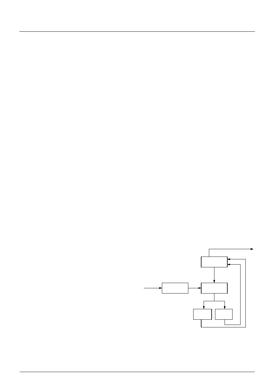
2.4. General Purpose Timer
The UAC 3553B incorporates a timer. It is a 16-bit
counter with clock prescaler. The clock is running at
12 MHz. The prescaler can be set to divide by 1...256.
The current value of the counter can always be read
back.
The timer initiates interrupts on reaching the count
value MaxA.
The structure of the timer is shown in Fig. 2�2.
Timer frequency:
Fig. 2�2: Timer structure
T
CLK
12MHz
Prescale
-----------------------
=
Prescaler
12 MHz
Counter
Max A
Max B
Control
Timer Interrupt
Tclk
UAC 3553B
DATA SHEET
8
May 21, 2003; 6251-595-1DSDS
Micronas
2.5. Audio Streaming Interface
The audio streaming interface directly connects the
USB interface to the APU in order to transmit the digi-
tal audio data for playback.The following data formats
are supported:
2.6. Audio Control Interface
The Audio Control Interface links the microcontroller to
the APU and is used to initialize the APU and to trans-
mit audio-related USB control data, like volume set-
ting, tone control, etc.
The Audio Control Interface supports full access to all
APU registers via the microcontroller.
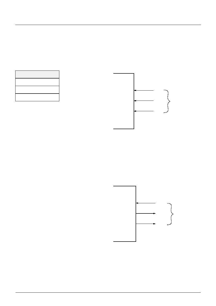
2.7. The I
2
S - Interface
Used Pins: DAI, WSI, CLI
The I
2
S interfaces operate in 16-bit or 32-bit mode.
Delayed word strobe or standard I
2
S format can be
selected via the programmable delay bit. Word strobe
polarity is programmable, also.
2.7.1. Asynchronous I
2
S input
Used Pins: DAI, WSI, CLI
In this mode the UAC 3553B is slave, i.e., asynchro-
nous input is possible at a sampling rate range from
6.4 kHz to 48 kHz. The external I
2
S source provides
DAI, WSI, and CLI
Fig. 2�3: Asynchronous I
2
S input
2.7.2. Synchronous I
2
S Input Mode
Used Pins: DAO, DAI, WSI, CLI
In this mode external digital sources use CLI and WSI
as reference and generate synchronous input data on
DAI.
Fig. 2�4: Synchronous I
2
S input
Table 2�1: Audio Formats
Playback
16-bit MONO
16-bit STEREO
24-bit STEREO
DAI
CLI
WSI
asynchronous
input
UA
C
355
3B
DAI
CLI
WSI
UAC
355
3B
synchronous
input

DATA SHEET
UAC 3553B
Micronas
May 21, 2003; 6251-595-1DSDS
9
2.8. Power Supply
The UAC 3553B has on-chip voltage regulators pro-
viding the optimal supply voltages for the analog and
digital sections, thus allowing to power the IC by the
USB bus supply lines, as well, as from external supply.
They also serve to reduce cross-talk and EMI.
For stable operation, all regulators need external
capacitors.
The regulators are
1. VREG:
3.4-V Regulator for USB-signaling (saving external
regulator)
2. AREG0:
3.5-V regulator for analog back-end
3. AREG1:
3.5-V regulator for analog circuitry apart from back-
end.
Reference voltage for analog signals:
SREF:
1.7-V (optional 2.3 V) reference voltage for analog cir-
cuitry.
Note: It is recommended that AVSS0/1, SGND and
VSS are connected. In certain applications,
however, it may be better to split signal ground
from the other grounds in order to reduce noise.
5-V Mode
If a higher output level is required, the IC can operate
in 5-V modus. In this case, the IC is powered from an
external 5-V supply: AVDD has to be connected to
AREG0 and AREG1 and SREF must be switched to
5-V mode.
2.9. I
2
C Bus Interface
Pins: SDA, SCL
The UAC 3553B is equipped with an I
2
C bus master/
slave interface. The bus format and timing follows the
original specification for I
2
C (The I
2
C Specification-
V2.1). It operates with 5-V signalling at 100 kHz or
400 kHz.
Both master and slave mode require support from the
microcontroller firmware.
2.9.1. I
2
C Master
This mode allows control of external I
2
C devices, like
EEPROMs, LCD-Displays etc. This interface is used to
download configuration data and firmware from an
EEPROM after power-up. The bus protocol (subad-
dressing and packet length) is defined by firmware and
therefore programmable.
Note: Micronas standard firmware (Section 4. "Firm-
ware" on page 16) provides support for
USB-to-I
2
C bridging, allowing control of I
2
C-
devices via USB.
2.9.2. I
2
C Slave
In I
2
C slave mode, the interface provides an interrupt
to the microcontroller after detecting the assigned I
2
C
address (0x48). The corresponding interrupt service
routine handles this request and interprets incoming
data according to the application.
One example of handling could provide full access to
all memory locations.
UAC 3553B
DATA SHEET
10
May 21, 2003; 6251-595-1DSDS
Micronas
2.10. Analog Output
Pins: OUTL, OUTR,
FOPL, FOPR, FOUTL, FOUTR, FINL, FINR
The analog output system comprises the stereo audio
DAC, analog filters, op amps for external out-of-band-
noise filters, analog volume, mute, and the output
amplifiers.
2.10.1. Digital-to-Analog Converters
The UAC 3553B uses two multi-bit sigma delta DACs
with high linearity and SNR better than 95 dBA.
2.10.2. Analog Filter
Pins: FOPL, FOPR, FOUTL, FOUTR, FINL, FINR
This block contains the op-amps for the optional ana-
log external out-of-band-noise filters. It is recom-
mended to use a second-order filter for the main chan-
nels (OUTL, OUTR) (see Section 6. "UAC 3553B
Applications" on page 36). It is possible to omit this fil-
ters and to save the external components. In this case,
the op-amp has to be switched off and the pins
FOOTL/R, FINL/R and FOPL/R must be connected.
The output signal will contain more out-of-band noise,
which is not audible, however.
2.10.3. Analog Volume
The analog volume covers a range from +6 dB to
-18 dB with 1.5 dB step size. But this is the analog
component of the overall volume system which covers
a range from +12 dB to
-
114 dB with 1 dB step size
and additional mute position. It is split into analog and
digital volume. This splitting ensures that the DAC per-
formance parameters do not degrade at reduced vol-
ume settings. The splitting is embedded in the audio
processing and cannot be modified.
Note: Positive volumes will degrade the THD at high
input levels.
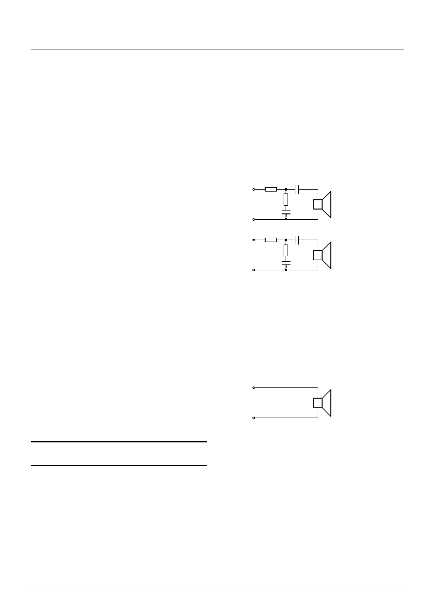
2.10.4.Line-out/Headphone Amplifier
Pins: OUTL, OUTR
Stereo Mode
The line-out/headphone amplifier output is provided at
the OUTL and OUTR pins connected either to stereo
headphones or to a power amplifier. The stereo head-
phones require external serial resistors in both chan-
nels. See Section 6. "UAC 3553B Applications" on
page 36.
Fig. 2�5: Loudspeaker connection for Stereo mode
Mono Mode
In Mono mode, the DC coupling capacitors and further
filter circuitry are not required. In this mode, the output
pins OUTL/R operate in bridge mode with complemen-
tary signals. Therefore, the maximum output power
increases allowing small speakers to be driven directly.
Fig. 2�6: Loudspeaker connection for Mono mode
OUTL
AVSS
OUTR
AVSS
OUTR
OUTL

DATA SHEET
UAC 3553B
Micronas
May 21, 2003; 6251-595-1DSDS
11
2.11.Special I/O
Pins: SOF, SEN, SUSPEND, RESET
The following sections describe some pins with special
functionality.
2.11.1.SOF (Start of Frame)
The SOF pin provides a 1-ms periodic signal which is
derived from the USB frame rate. It can be used for
test purpose or as an USB-synchronous reference for
vendor-specific external circuitry.
2.11.2.SEN (Suspend Enable)
Pin: SEN
This is a digital input that prevents the device from
entering the low-power mode (Suspend). The
UAC 3553B enters a low power mode if:
� J-state on D+, D
-
lines (USB-Suspend) and Vbus
high
� Vbus low (USB-disconnected)
Note: Both cases must be supported by the firmware
In case of USB-Suspend, the SEN pin is also used as
an input for the remote wake-up function.
2.11.3.Suspend
Pin: SUSPEND
The SUSPEND pin is a digital output pin which indi-
cates the low-power mode. It can be used to power
down external circuitry, like power amplifiers in an USB
speaker.
2.11.4.Reset
Pin: RES
The RES pin resets the UAC 3553B. During power up
the RES pin should be low until the clock system is up
and running. Then this pin can be released and the
UAC 3553B enters normal operating mode.
Note: In low-power mode, the RES pin must not be
low to avoid restart of the clock system and
therefore entering normal power mode.
Fig. 2�7: Timing diagram of the reset procedure
2.12.Clock System
Pins: XTI, XTO
The UAC 3553B requires a 12-MHz clock source,
which is realized as an on-chip oscillator with external
crystal. Also an external oscillator can be used. In this
case, the clock has to be connected to XTI (see also
Section 6.2. "External Clocking via XTI" on page 36).
The 12 MHz is the input clock for a PLL circuit which
generates all clocks needed within the IC.
The clock for the APU is programmable either to
48 MHz or 72 MHz. In case of 48 kHz, the UAC 3553B
consumes less power, but on the other hand a reduced
feature set for the audio processing has to be taken
into account (see Fig. 3�1 on page 12).
Table 2�2: SEN pin
SEN
high
suspend enabled
low
suspend disabled/remote wake-up
Table 2�3: SUSPEND pin
SUSPEND
high
normal power
low
low power
20 ms
90%
AVDD
RES
VDD
U
A
C
3
5
5
3
B
D
A
T
A
S
H
E
E
T
12
Ma
y 21,
2
003;
6251-595-1D
S
M
i
c
r
o
nas
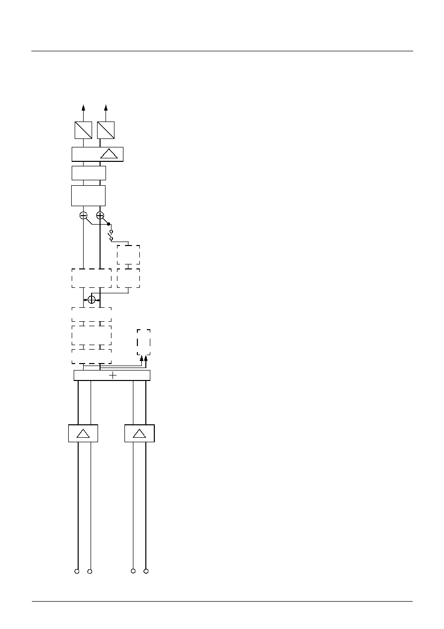
3. Audio Processing
Fig. 3�1: Signal flow in the audio processing unit (APU)
USB
mix
I
2
S
mix
USB
I
2
S
AGC
Bass/
Treble/
EQ
Comple-
mentary
High
Low
MDB
Loud-
ness
Vol.
B
a
l
ance
Q-Peak
(downstream)
D
A
Pass
Pass
D
A
L
L
R
R
Mono/
Stereo
+
Right
Invert
dashed blocks not available in reduced feature set
DATA SHEET
UAC 3553B
Micronas
May 21, 2003; 6251-595-1DS
13
The audio processing is realized by APU firmware.
The audio building blocks can be split into USB-inde-
pendent features such as parametric equalizer, I
2
S
I/O, and blocks which belong to USB feature units,
mixer units, and selection units defined in the USB
Device Class Definition for Audio Devices.
The USB feature unit provides basic manipulation of
the incoming logical channels and can be controlled by
the standard OS-provided mixer tool. The parameters
for the USB-independent features are predefined in
the internal ROM, in an external EEPROM or a special
host application which drives the IC.
The UAC 3553B supports two logical channels (i.e. left
and right). Multichannel or surround systems, how-
ever, can also be realized using more than one
UAC 3553B, because phase or delay distortion is elim-
inated in the device by locking the audio processing to
the USB frame rate. An overview of the architecture is
given in Fig. 3�1 on page 12.
If the APU works with a 48 MHz clock it is necessary to
select the reduced feature mode. The blocks, which
are not available in reduced feature mode are shown
with dashed lines in Fig. 3�1 on page 12.
3.1. Automatic Gain Control
The Automatic Gain Control (AGC) is one of the build-
ing blocks of the feature unit (USB Device Class Defi-
nition for Audio Devices 1.0, page 39).
Different sound sources fairly often do not have the
same volume level. The Automatic Gain Control solves
this problem by equalizing the volume levels within a
defined range. Below a threshold level the signals are
not affected. The level-adjustment is performed with
time constants in order to avoid short-time adjustments
due to signal peaks.
Fig. 3�2: Simplified AGC characteristics
3.2. Quasi-Peak
A quasi-peak detector is provided in the DAC channel.
This can be used e.g. for a VU-meter on the host side.
The feature is based on using fast attack and slow
decay time constants.
3.3. Bass Control
The bass control provides gain or attenuation to fre-
quency components below a corner frequency of
120 Hz. The bass control works identically on both
channels in a range of
-
12 dB to +12 dB.
3.4. Treble Control
The treble control provides gain or attenuation to fre-
quency components above a corner frequency of
6 kHz. The treble control works identically on both
channels in a range of
-
12 dB to +12 dB.
Table 3�1: AGC parameters
Parameter
Settings
Default
Decay time
8 sec
4 sec
2 sec
20 ms
4 sec
-
30
-
24
-
18
-
12
-
6
+
6
Input Level
-
15
-
21
-
9
Output Level
dBr
dBr
0
AGC off
AGC on
UAC 3553B
DATA SHEET
14
May 21, 2003; 6251-595-1DS
Micronas
3.5. Parametric Equalizer
The parametric equalizer is an audio feature which is
not accessed via standard USB controls. It allows the
compensation of the frequency response of a speaker.
Alternatively, frequency responses can be set to suit
individual tastes. The equalizer consists of five individ-
ually adjustable bands. The control parameters and
the parameter range for each band is shown in Table
3�2.
The adjustment of the equalizer is supported by an
application program that allows to set up frequency
responses and to download the corresponding filter
coefficients into the UAC 3553B. When the frequency
response matches the requirements, it can be pro-
grammed into the external EEPROM or can be set by
a vendor specific device driver. The UAC 3553B is
shipped with a flat frequency response.
3.6. Volume, Mute, and Balance Control
The volume control is partly realized in the analog
back-end. This preserves high audio quality (SNR) at
low volume settings because signal and noise are
attenuated in the same way. This is a significant
advantage over digital-only implemenations since it
preserves the native audio bit resolution in the pro-
cessing path. The UAC 3553B uses digital volume
control only for the fine stepping. The volume setting is
smoothed by an internal ramping algorithm in order to
avoid audible clicks during volume change. The split-
ting between analog and digital volume is handled by
the UAC 3553B automatically.
The balance is implemented digitally by attenuating
one channel.
The mute control is part of the volume system in the
UAC 3553B. It functions simultaneously on both chan-
nels and can be switched on and off under USB con-
trol. Similar to the volume control, clicks are avoided
by a ramping algorithm.
3.7. Micronas Dynamic Bass (MDB)
The Micronas Dynamic Bass algorithm (MDB) imple-
ments a sophisticated bass boost system, which
extends the frequency range of loudspeakers or head-
phones.
The MDB is placed in the crossover filter path. The
enhanced bass signal can be added back onto the
left/right channels. Micronas Dynamic Bass combines
two effects: dynamic amplification and adding harmon-
ics.
Several parameters allow tuning the characteristics of
MDB according to the loudspeaker, the cabinet, and
personal preferences. For more detailed information
on how to set up MDB, Micronas provides an appropri-
ate Application Note.
Table 3�2: Equalizer parameters
Parameter
Min
Max
Center Frequency
50 Hz
15 kHz
Gain/Attenuation
-
6 dB
+6 dB
Filter Quality (Q)
0.5
3
Table 3�3: MDB parameters
Parameter
Range
Default if
disabled
Default if
enabled
Effect
Strength
off...max
off
medium
Harmonic
Content
0...100%
0%
50%
Center Fre-
quency
20...300 Hz
90 Hz
90 Hz
Amplitude
Limit
-
32 ...0
dBFS
0 dBFS
(=no limit)
0 dBFS
(=no limit)
DATA SHEET
UAC 3553B
Micronas
May 21, 2003; 6251-595-1DS
15
3.7.1. Dynamic Amplification
Since the human impression of loudness depends on
the frequency, a dynamic compression of the low fre-
quencies adapts the sound to the human perception.
In order to prevent clipping and to adapt the system to
the signal amplitude which is really present at the out-
put of the device, the MDB contains a definable limit.
The output signal amplitude is monitored and if it
comes close to the limit, the gain is reduced automati-
cally. Clipping effects are avoided.
Fig. 3�3: Dynamic amplification
3.7.2. Adding Harmonics
MDB exploits the psychoacoustic phenomenon of the
`missing fundamental'. Adding harmonics of the fre-
quency components below the cutoff frequency gives
the impression of actually hearing the low frequency
fundamental. In other words: Although the loud-
speaker system is not capable of generating such low
frequencies, the listener has the impression that it
reproduces them.
Fig. 3�4: Adding harmonics
Frequency
MDB_LIMIT
MDB_CF
S
i
gna
l
Level
A
m
p
litu
d
e
SUBW_FREQ
(db)
Frequency
MDB_CF
A
m
pl
i
t
ud
e (db
)
UAC 3553B
DATA SHEET
16
May 21, 2003; 6251-595-1DS
Micronas
4. Firmware
It was the purpose of the previous chapters to describe
the UAC 3553B from the hardware point of view. The
complete functionality, however, is defined by the
microcontroller firmware. This firmware tailors the
device to a specific application. Micronas offers a stan-
dard DAC firmware versions which is embedded in the
ROM.
Note: By means of an external EEPROM it is possible
to customize many parameters (IDs, strings,
equalizer setting etc.).
4.1. Features
The main features of the standard firmware versions
are
� USB playback withsample rates from 6.4 kHz to
48 kHz
� Audio baseband processing incl. dynamic bass
management
� Basic audio control by GPIO-HID
� Suspend mode and remote wake-up support
� I�C master/slave support
� bootloader allows download of configuration data,
plug-ins after power-on
� plug-in support (downloadable firmware extensions
from external EEPROM or WIN driver)
Most of the functionality is defined in the device and
configuration descriptor. The following chapters pro-
vide all noteworthy information, which is buried in this
descriptors. It is assumed that the reader is familiar
with the basic USB notation (USB Spec 1.1 etc.).
4.1.1. Device Descriptor
The device descriptor contains the downloadable IDs
and the index for the strings.
Associated to the string index there are three program-
mable strings. The ROM firmware defines only two:
4.1.2. Configuration Descriptor
First the configuration descriptor contains information
on the bus/self-powered and remote wake-up capabili-
ties. The UAC 3553B allows all combinations of these
features. There is also a string index, allowing to asso-
ciate a string to this configuration. The default string is
the date code (time of code assembly). These items
are programmable.
Table 4�1: Programmable Device Descriptor Items
Item
Default - UAC 3553B
idVendor
0x074D
idProduct
0x3553
bcdDevice
0x000x
1)
iManufacturer
0x01
iProduct
0x02
iSerialNumber 0x00
1)
changes with new firmware revisions
Table 4�2: Strings used in DAC Firmware
String
Default - UAC3553B
Manufacturer String
Micronas
Product String
UAC3553B USB-DAC
Table 4�3: Programmable Configuration Descriptor
Items
Item
Default - UAC3553B
iConfig
0x01
bmAttributes
0xC0 (self-powered,
remote wake-up
MaxPower
0x00 (0mA)
DATA SHEET
UAC 3553B
Micronas
May 21, 2003; 6251-595-1DS
17
Then the configuration descriptor provides all informa-
tion concerning the audio flow in the Class Specific
Audio Control Interface. Fig. 4�1 shows the graphical
representation for the DAC firmware.
This are the audio structure how it appears to the USB
host. Without any additional drivers the Windows OS
provides sliders in the mixing tool to control volume,
bass, treble setting. Using a vendor-specific applica-
tion, however, it is possible to extend this to the full sig-
nal routing capabilities (see Section 3. on page 12).
can be achieved by plug-ins from external EEPROM or
Windows driver.
Note: BassBoost enables a dynamic bass manage-
ment algorithm with programmable (ext.
EEPROM) characteristics.
The next part of the configuration descriptor defines
the audio format for playback. This is not programma-
ble.
The UAC 3553B accepts all sample rates from 6.4 kHz
to 48 kHz
The final portion of the configuration descriptor defines
the HID functions:
The DAC firmware uses the GPIO pins to connect
keys which are related to the USB HID class. The
standard configuration defines the GPIO0 ...GPIO7 as
input pins for the audio and media control shown in
Table 4�5.
The keys are polled every 1 ms by the microcontroller
and the corresponding key codes are transmitted to
the host on request when a key enters high state. The
hosts polling rate is 8 ms. This parameter, however, is
part of the configuration set, which can be downloaded
from an external I
2
C-EEPROM.
If this HID functions are not required the GPIO[0...7]
can be used as general-purpose I/O by vendor specific
applications.
4.1.3. Audio Class Requests
The DAC firmware supports all audio class requests
which are required by the audio flow shown in Fig. 3�
1. The MIN/MAX/RES setting follows the limits which
are defined in the audio processing apart from the
main volume setting (FU1). In this case, the overall
range from
-
114 dB to +6 dB is limited to
-
40 dB to
+3 dB (plus mute position) in order to fit the audible
range to the volume slider in the Windows mixer.
Fig. 4�1: Standard DAC audio flow
Table 4�4: Supported Audio Formats
Playback Format
16-bit MONO
16-bit STEREO
24-bit STEREO
Table 4�5: Standard Key Configuration
Pin
Function
GPIO0
Volume Up
GPIO1
Volume Down
GPIO2
Mute on-off toggle
GPIO3
BassBoost on-off toggle
GPIO4
Next Track
GPIO5
Previous Track
GPIO6
Stop
GPIO7
Playback
IT
EP1
USB
ID12
FU
Volume,Mute,
Bass,Treble
BassBoost
AGC
ID1
OT
ID14
D/A
Playback
UAC 3553B
DATA SHEET
18
May 21, 2003; 6251-595-1DS
Micronas
4.2. Vendor-Specific Requests
These requests provide functionality which extents
standard controlling of the operating system. Micronas
provides a driver for Windows operating systems
which supports:
� SET MEM
This request allows to write all RAM and register
locations in the chip.
� GET MEM
This request allows to read all memory locations in
the chip. Block read is supported
� SET I
2
C
This vendor request allows to drive the I
2
C-master
in the DAC firmware. It allows to write to external
I
2
C devices
� GET I
2
C
This request supports I
2
C master reading from
external devices
4.2.1. Bootloader
The bootloader is a part of the firmware which allows
communication with an external I
2
C EEPROM. In
multi-master applications with I
2
C control, however, it
is not allowed to have I
2
C traffic coming from
UAC 3553B and therefore, the bootloader needs to be
enabled by GPIO7:
The bootloader runs immediately after power-on. At
this time the device is not connected to the USB bus.
When the bootloader has finished, the pull-up resistor
is switched on the D+ line to signal the host that the
device is ready for ennumeration. If no external
EEPROM is found, the UAC 3553B continues with the
default configuration. Two I
2
C-EEPROM types with dif-
ferent I
2
C-device IDs and number of subaddresses are
supported and can be selected by GPIO6. The
EEPROM type and size must be choosen according to
the content.
The size of the EEPROM must be chosen according to
the content.
Details on the EEPROM content and the structure of
the different sections can be found in separate applica-
tion notes.
Note: Using GPIO6/7 as bootloader option bits may
cause conflicts with the use of this pins as HID
media control pins. In this case, a plug-in or a
hardware workaround is available
Table 4�6: Bootloader enable
Setting
Bootloader
GPIO7 = 0
disabled
GPIO7 = 1
enabled
Table 4�7: Supported I
2
C EEPROM types
GPIO6
Device
ID
Sub-
addresses
Size
Purpose
1
0x51
1 Byte
<2 kbit
Configuration
(and very
small plug-
ins)
0
0x50
2 Bytes
>2 kbit
Configuration
and plug-ins
DATA SHEET
UAC 3553B
Micronas
May 21, 2003; 6251-595-1DS
19
5. Specifications
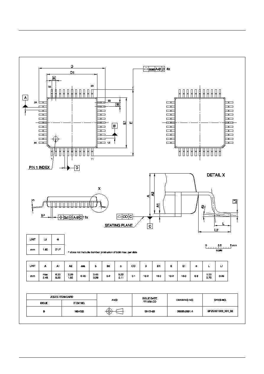
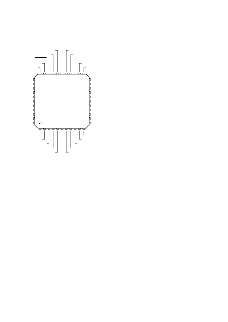
5.1. Outline Dimensions
Fig. 5�1:
PMQFP44-1: Plastic Metric Quad Flat Package, 44 leads, 10
�
10
�
2 mm
3
Ordering code: QG
Weight approximately 0.5 g
UAC 3553B
DATA SHEET
20
May 21, 2003; 6251-595-1DS
Micronas
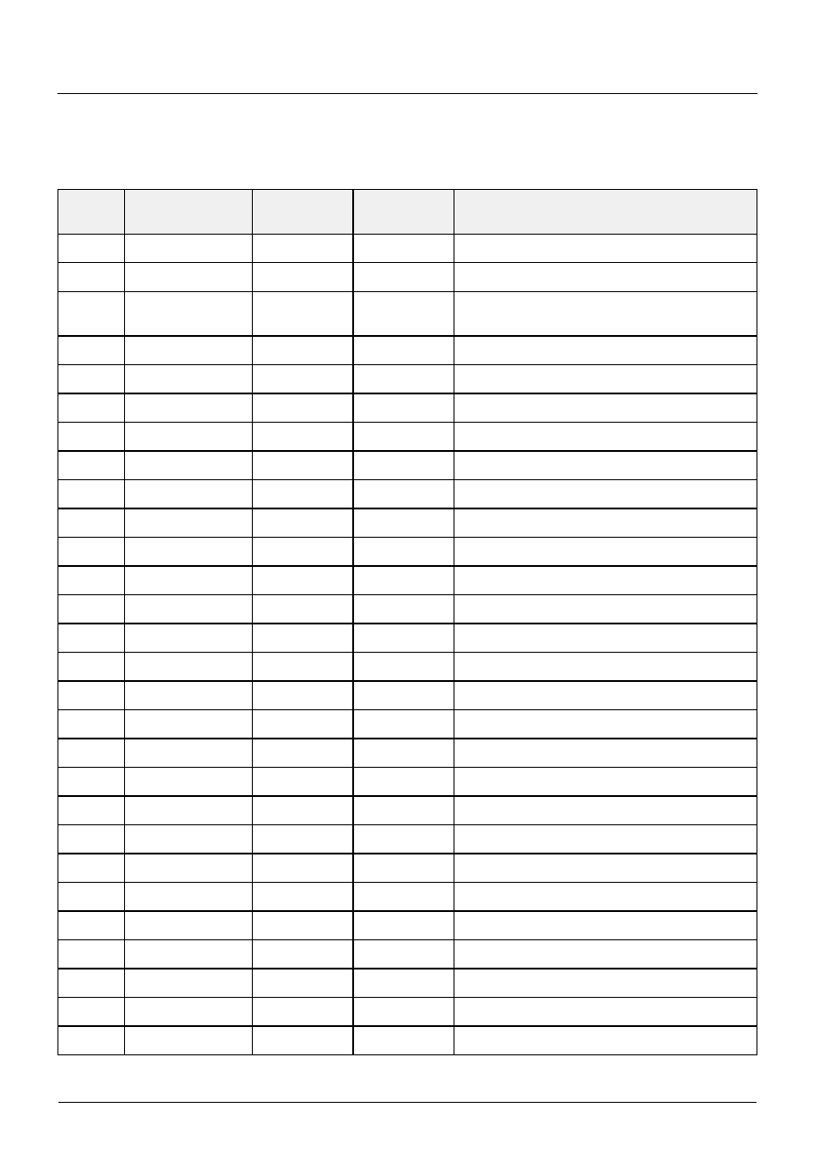
5.2. Pin Connections and Short Descriptions
NC = not connected, leave vacant
LV
= if not used, leave vacant
VSS = if not used, connect to VSS
OBL = obligatory; connect as described in
circuit diagram
VDD = connect to VDD
Pin No.
Pin Name
Type
Connection
(If not used)
Short Description
1
XTI
IN
OBL
Quartz Oscillator Pin 1
2
XTO
OUT
OBL
Quartz Oscillator Pin 2
3
AREG1
OUT
OBL
Regulator Output for analog parts except
amplifiers
4
AVSS1/AVSS0
IN
OBL
VSS for analog parts
5
OUTL
OUT
LV
Audio Output: headphone left / speaker Left
6
OUTR
OUT
LV
Audio Output: headphone right /speaker Right
7
AREG0
OUT
OBL
Regulator Output for audio output amplifiers
8
AVDD
IN
OBL
analog VDD
9
DAI
IN
VSS
I
2
S Data Input
10
WSI
IN/OUT
VSS
I
2
S Word Strobe
11
CLI
IN/OUT
VSS
I
2
S Bit Clock
12
GPIO 7
IN/OUT
LV
HID IO 7
13
GPIO 6
IN/OUT
LV
HID IO 6
14
GPIO 5
IN/OUT
LV
HID IO 5
15
GPIO 4
IN/OUT
LV
HID IO 4
16
GPIO 3
IN/OUT
LV
HID IO 3
17
GPIO 2
IN/OUT
LV
HID IO 2
18
GPIO 1
IN/OUT
LV
HID IO 1
19
GPIO 0
IN/OUT
LV
HID IO 0
20
SDA
IN/OUT
LV
I
2
C Data
21
SCL
IN/OUT
LV
I
2
C Clock
22
TRDY
OUT
LV
Test Output Pin
23
VBUS
IN
OBL
Sense USB Bus
24
VREG
OUT
OBL
Capacitor for internal supply
25
DMINUS
IN/OUT
OBL
USB DATA MINUS
26
DPLUS
IN/OUT
OBL
USB DATA PLUS
27
VSS
IN
OBL
Digital VSS
28
VDD
IN
OBL
Digital VDD
DATA SHEET
UAC 3553B
Micronas
May 21, 2003; 6251-595-1DS
21
29
TEST
IN
VSS
Test Enable
30
RES
IN
VDD
Power On Reset, active low
31
SUSPEND
OUT
LV
Low-Power Mode Indicator
32
SOF
OUT
LV
1-ms Start-Of-Frame Signal
33
SEN
IN
VSS
Suspend Enable
34
FOUTL
OUT
OBL
Output to left external filter
35
FOPL
IN/OUT
OBL
Filter Op Amp Inverting Input, left
36
FINL
IN/OUT
OBL
Input for FiltoutL
37
FOUTR
OUT
OBL
Output to right filter op amp
38
FOPR
IN/OUT
OBL
Right Filter op amp inverting input
39
FINR
IN/OUT
OBL
Input for FILTOUTR
40
NC
LV
Leave Vacant
41
NC
LV
Leave Vacant
42
SGND
IN
OBL
Signal Reference Ground
43
SREF
IN
OBL
Signal Reference Voltage
44
NC
LV
Leave Vacant
Pin No.
Pin Name
Type
Connection
(If not used)
Short Description

UAC 3553B
DATA SHEET
22
May 21, 2003; 6251-595-1DS
Micronas
5.3. Pin Descriptions
5.3.1. Power Supply Pins
The UAC 3553B combines various analog and digital
functions which may be used in different modes. For
optimized performance, major parts have their own
power supply pins. All VSS power supply pins must be
connected.
VDD (28)
VSS (27)
The VDD and VSS power supply pair are connected
internally with all digital parts of the UAC 3553B.
AVDD (8)
AVDD is the supply pin for the voltage regulators at
AREG0(9) and AREG1(4).
AVSS0/1 (4)
AVSS1 is the ground connection for the analog audio
processing parts, including the headphone/loud-
speaker amplifiers.
SREF (43)
Reference for analog audio signals. This pin is used as
reference for the internal op amps. This pin must be
blocked against SGND with a 3.3-
�
F capacitor.
Note: The pin has a typical DC level of 1.725 V. It can
be used as reference input for external op amps
when no current load is applied.
SGND (42)
Reference ground for the internal band-gap and bias-
ing circuits. This pin should be connected to a clean
ground potential! Any external distortions on this pin
will affect the analog performance of the UAC 3553B.
AREG0 (7)
Voltage regulator output for headphone/loudspeaker
amplifiers supply. Connect an external ceramic capaci-
tor to stabilize the regulator output.
AREG1 (3)
Voltage regulator output for analog audio processing
parts supply, except the headphone/loudspeaker
amplifiers. Connect an external ceramic capacitor to
stabilize the regulator output.
5.3.2. Analog Audio Pins
FOUTL (34)
FOPL (35)
FINL (36)
FOUTR (37)
FOPR (38)
FINR (39)
Filter op amps are provided in the analog baseband
signal paths. These inverting op amps are freely
accessible for external use by these pins.
The FOUTL/R pins are connected with the buffered
output of the internal switch matrix. The FOPL/R pins
are directly connected with the inputs of the inverting
filter op amps. The FINL/R pins are connected to the
outputs of the op amps.
OUTL (5)
OUTR (6)
These pins are connected to the internal output ampli-
fiers. OUTL/R can be used for either line-out or stereo
headphones.
Caution: A short-circuit at these pins for more than a
momentary period may result in destruction of the
internal circuits.

DATA SHEET
UAC 3553B
Micronas
May 21, 2003; 6251-595-1DS
23
5.3.3. Interface Pins
DMINUS (25)
DPLUS (26)
Differential USB port pins. The DPLUS pin has an
internal switchable pull-up resistor. Both pins must be
connected to the USB bus via a series resistor.
VBUS (23)
Sense USB Bus.
CLI (11)
Clock line for the I
2
S bus. This line is driven by the
UAC 3553B; in slave mode, an external I
2
S clock has
to be supplied.
DAI (9)
Input of digital serial sound data to the UAC 3553B via
I
2
S bus.
WSI (10)
Word strobe line for the I
2
S bus. In master mode, this
line is driven by the UAC 3553B; in slave mode, an
external I
2
S word strobe has to be supplied.
SDA (20)
Via this pin, the I
2
C bus data is written to or read from
the UAC 3553B.
SCL(21)
Via this pin, the I
2
C bus clock signal has to be sup-
plied.
5.3.4. Other Pins
XTI (1)
XTO (2)
The XTI pin is connected to the input of the internal
crystal oscillator; the XTO pin to its output. Both pins
should be directly connected to the crystal and two
ground-connected capacitors (see application dia-
gram).
Note: Do not drive external clock circuits via XTI/XTO.
SEN (33)
Digital input that prevents the device from entering the
low-power mode. This pin is also used to signal remote
wake-up.
TEST (29)
Test enable. This pin is for test purposes only and
must always be connected to VSS.
VREG (24)
Voltage regulator output for USB transceiver supply.
Connect an external ceramic capacitor to stabilize the
regulator output.
RES (30)
A Low signal at this pin resets the chip.
GPIO 0...7
(19, 18, 17, 16, 15, 14, 13, 12)
These pins are configurable to be either input or output
and can be used to connect audio function keys or sig-
nalling LEDs.
SUSPEND (31)
This pin indicates that the host PC sets the USB bus to
the suspend mode state.
SOF(32)
Start of Frame Signal. 1-ms signal that can be used for
external application circuits.
TRDY (22)
Test Output Pin. This pin is intended for test purposes
only and must not be connected.
UAC 3553B
DATA SHEET
24
May 21, 2003; 6251-595-1DS
Micronas
5.4. Pin Configuration
Fig. 5�2: PMQFP44-1 package
34
35
36
37
38
39
40
41
42
43
44
22
21
20
19
18
17
16
15
14
13
12
1
2
3
4
5
6
7
8
9
10 11
33 32 31 30 29 28 27 26 25 24 23
UAC 3553B
SEN
SOF
SUSPEND
RES
TEST
VBUS
VREG
DMINUS
DPLUS
VSS
NC
SREF
SGND
NC
NC
FINR
FOPR
FOUTR
FINL
FOUTL
FOPL
GPIO 7
GPIO 6
GPIO 5
GPIO 4
GPIO 3
GPIO 2
GPIO 1
GPIO 0
SDA
TRDY
SCL
XTI
XTO
AREG1
AVSS1/AVSS0
OUTL
CLI
WSI
DAI
AVDD
AREG0
OUTR
VDD
DATA SHEET
UAC 3553B
Micronas
May 21, 2003; 6251-595-1DS
25
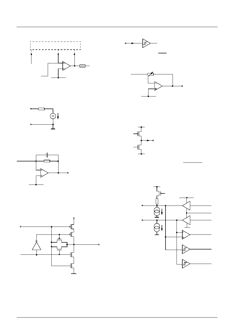
5.5. Pin Circuits
Fig. 5�3: Pins FINR, FOPR, FINL, FOPL
Fig. 5�4: Pins SREF, SGND
Fig. 5�5: Output Pins FOUTL, FOUTR
Fig. 5�6: Clock oscillator XTI, XTO
Fig. 5�7: Input Pins RES, TEST, SEN, DAI
Fig. 5�8: Output Pins OUTL, OUTR
Fig. 5�9: Digital Output Pins SOF, SUSPEND, TRDY
Fig. 5�10: Digital Input/Output Pins DMINUS,
DPLUS, VREG
SREF
FOPn
FINn
FOUTn
ext. filter network
115 k
SREF
SGND
SREF
FOUTn
AREG1
AVSS0/1
P
P
P
N
N
N
XTO
XTI
Enable
OUTn
SREF
DV
SUP
P
N
GND
DPLUS
DMINUS
VREG
VSS
P
VREG
1.5 k
UAC 3553B
DATA SHEET
26
May 21, 2003; 6251-595-1DS
Micronas
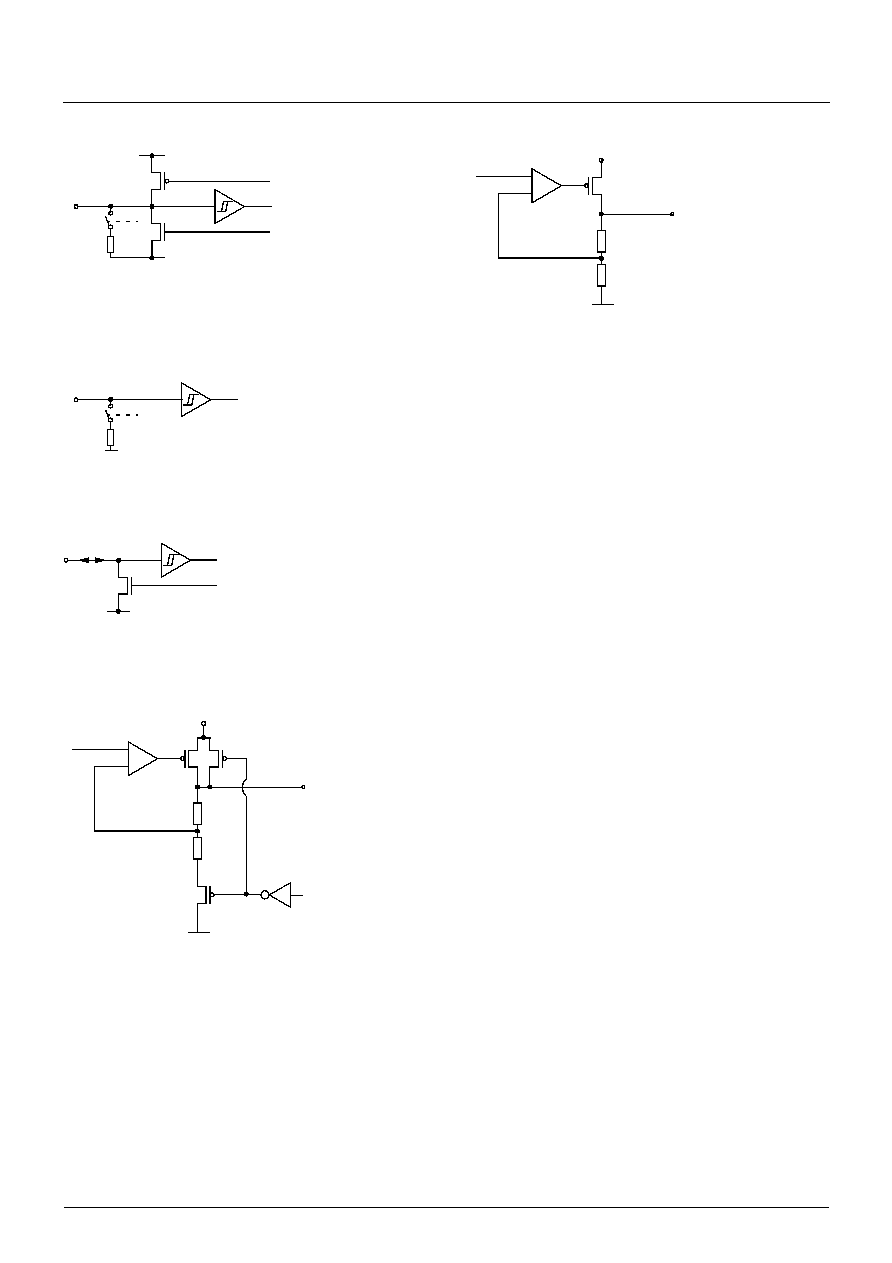
Fig. 5�11: Input/Output Pins GPIO0... GPIO7, WSI,
CLI
Fig. 5�12: Input Pin VBUS
Fig. 5�13: Input/Output Pins SDA, SCL
Fig. 5�14: Analog Voltage Supply Pins AVDD, AVSS,
AREG0/1
Fig. 5�15: Digital Voltage Supply Pins VDD, VSS,
VREG
DV
SUP
P
N
GND
N
GND
AREG0/1
-
AVDD
AVSS0/1
+
Suspend
VREG
-
VDD
VSS
+
DATA SHEET
UAC 3553B
Micronas
May 21, 2003; 6251-595-1DS
27
5.6. Electrical Characteristics
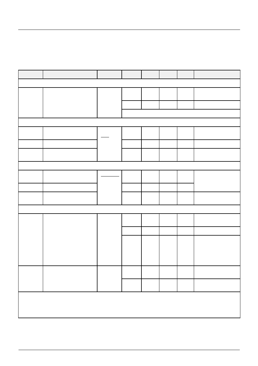
5.6.1. Absolute Maximum Ratings
Stresses beyond those listed in the "Absolute Maximum Ratings" may cause permanent damage to the device. This
is a stress rating only. Functional operation of the device at these or any other conditions beyond those indicated in
the "Recommended Operating Conditions/Characteristics" of this specification is not implied. Exposure to absolute
maximum ratings conditions for extended periods may affect device reliability.
Symbol
Parameter
Pin
Name
Min.
Max.
Unit
T
A
Ambient Operating Temperature
0
70
�
C
T
C
Case Operating Temperature
0
110
�
C
T
S
Storage Temperature
-
40
125
�
C
P
tot
Power Dissipation
-
650
mW
V
SUPA
Analog Supply Voltage
1)
AVDD
-
0.3
6
V
V
SUPA
Analog Supply Voltage
2)
AVDD,
AREG0/1
-
0.3
6
V
V
SUPDx
Digital Supply Voltage
VDD
-
0.3
6
V
V
GRND
Voltage Differences between
different Grounds
AVSS0,
AVSS1,
VSS
-
0.5
+0.5
V
V
Idig
Input Voltage, all digital inputs
-
0.3
V
SUPD
+ 0.3
V
I
Idig
Input Current, all digital inputs
4)
-
20
+20
mA
I
Odig
Output Current, all digital outputs
-
50
+50
mA
V
Iana
Input Voltage, all analog inputs
-
0.3
V
VAREG0/1
+ 0.3
V
I
Iana
Input Current, all analog inputs
4)
-
5
+
5
mA
I
Oaudio
Output Current, audio output
3)4)
OUTL/R
-
0.2
0.2
A
I
AREG0
Output Current, analog regulator
4)
AREG0
-
500
+20
mA
I
AREG1
Output Current, analog regulator
4)
AREG1
-
50
+20
mA
1)
Internal regulators used
2)
If internal regulators are not used, connect AVDD to AREG0/1.
3)
These pins are not short-circuit proof!
4)
Positive value means current flowing into the circuit
UAC 3553B
DATA SHEET
28
May 21, 2003; 6251-595-1DS
Micronas
5.6.2. Recommended Operating Conditions
Symbol
Parameter
Pin Name
Min.
Typ.
Max.
Unit
Temperature Ranges and Supply Voltages
T
A
Ambient Temperature Range
0
70
�
C
V
SUPA
Analog Audio Supply Voltage
AVDD
4.1
5.0
5.6
V
C
SUPA
Capacitor at analog supply pins to
ground
AVDD
220
nF
V
SUPD
Digital Supply Voltage
VDD
4.1
5.0
5.6
V
C
SUPD
Capacitor at digital supply pin to
ground
VDD
100
nF
C
SUPUSB
Capacitor at VBUS pin to ground
VBUS
22
nF
Analog Reference
C
SREF1
Analog Reference Capacitor
SREF
1
3.3
�
F
C
SREF2
Ceramic Capacitor in parallel
SREF
100
nF
Analog Audio Filter Inputs and Outputs
Z
AFLO
Analog Filter Load Output
1)
FOUTL/R
7.5
6
k
pF
Z
AFLI
Analog Filter Load Input
1)
FINL/R
5.0
7.5
k
pF
Analog Audio Outputs
Z
AOL_HP
Output Load Headphone
(16-
series resistor required)
OUTL/R
16
32
100
pF
1)
Please refer to Section 6. "UAC 3553B Applications" on page 36
DATA SHEET
UAC 3553B
Micronas
May 21, 2003; 6251-595-1DS
29
Crystal Characteristics
1)
T
AC
Ambient Temperature Range
0
70
�
C
F
P
Load Resonance Frequency
at C
load
= 22 pF
2)
XTI
12
MHz
V
ACLK
Clock Amplitude
XTI, XTO
0.5
V
REG
-
0.5
1)
V
PP
F/F
s
Accuracy of Adjustment
-
500
500
ppm
F/F
s
Frequency Variation
versus Temperature
-
500
500
ppm
R
EQ
Equivalent Series Resistance
12
30
C
0
Shunt (parallel) Capacitance
3
5
pF
Voltage Regulator
C
VREG
Voltage Regulator Capacitor
(ceramic, X5R)
VREG
330
1000
nF
C
AREG0
Voltage Regulator Capacitor
(ceramic, X5R)
AREG0
330
470
600
nF
C
AREG1
Voltage Regulator Capacitor
(ceramic, X5R)
AREG1
150
220
270
nF
Transceiver
R
USB
Input Series Resistance
DPLUS/
DMINUS
24
(
�
5%)
1)
For device characteristics refer to page 30
2)
C
load
should be typically 22 pF (+30%/
-
10%) e. g. Y5U. Ref. to application circuit (see Fig. 6.3. on page 37)
Symbol
Parameter
Pin Name
Min.
Typ.
Max.
Unit
UAC 3553B
DATA SHEET
30
May 21, 2003; 6251-595-1DS
Micronas
5.6.3. Characteristics
At T
A
= 0 to 70
�
C, V
SUPD
= 4.1 V to 5.6 V, V
SUPA
= 4.1 V to 5.6 V. Typical values at T
A
= 20
�
C,
V
SUPD
= V
SUPA
= 5.0 V, quartz frequency = 12 MHz, duty cycle = 50%, bass/treble: 0 dB, Micronas Dynamic Bass:
off, AGC: off, equalizer: off (positive current flowing into the IC), 3-V Mode, reduced feature set, if not otherwise
specified.
Symbol
Parameter
Pin Name
Min.
Typ.
Max.
Unit
Test Conditions
Digital Supply
I
VDD
Current Consumption
1)
VDD
57
45
70
mA
72 MHz APU clock
48 MHz APU clock
30
80
�
A
Suspend
Digital Input Pin
I
I
Input Leakage Current
GPIO[7:0],
SEN,
RES,
VBUS,
DAI, WSI,
CLI
�
1
�
A
V
GND
V
I
V
SUP
V
IL
Input Low Voltage
0.4
V
V
IH
Input High Voltage
V
SUPD
-
0.4V
V
Digital Output Pin
V
OH
Output High Voltage
GPIO[7:0]
SUSPEND,
SOF, WSI,
CLI, SDA,
SCL
V
SUPD
-
0.4
V
Pins set to output
I
out
=8 mA
V
OL
Output Low Voltage
0.4
V
I
O_max
Max. Output Current
1
3)
8
2)3)
mA
output set to "weak"
output set to "strong"
Analog Supply
I
AVDD
Current Consumption
Analog Audio
AVDD
12
15
mA
all analog blocks on,
Mute
120
135
�
A
Suspend
25
mA
R
L
32
(external 16-
series
resistor required)
Volume = 0 dB,
Input signal 1kHz at
0 dB
FS
PSRR
AA
Power Supply Rejection
Ratio for Analog Audio
Outputs (internal regulators
active)
AVDD,
OUTL/R
95
dB
1 kHz sine wave at
100 mV
rms
55
dB
100 kHz sine wave at
100 mV
rms
1)
no load attached to GPIOs
2)
max output current for driving LEDs is 20 mA.
3)
the sum of these digital output pin currents must not exceed 100 mA. Higher currents might damage the device.
Please consider power limitations due to USB specification.
DATA SHEET
UAC 3553B
Micronas
May 21, 2003; 6251-595-1DS
31
Analog Supply Voltage Regulators
V
AREG
Output Voltage
AREG0/1,
AVSS0/1
3.3
3.5
3.7
V
Reference Frequency Generation
V
DCXTI
DC Voltage at Oscillator
Pins
XTI/O
0.5*
V
Areg1
V
C
LI
Input Capacitance at
Oscillator Pin
XTI
3
pF
C
LO
Input Capacitance at
Oscillator Pin
XTO
3
pF
V
XTALOUT
Voltage Swing at Oscillator
Pins (peak-peak)
XTI/O
0.6 *
V
Areg1
1.0 *
V
Areg1
V
T
OSC_rise
Oscillator Start-Up Time
10
ms
after min. V
SUPA
is
reached
USB Transceiver
V
REG
Regulator Voltage
VREG
3.25
3.4
3.55
V
C
L
=1
�
F
R
O
Driver Output Resistance
including the 24-
external
serial resistor
D+/D
-
28
43
static, LOW or HIGH
t
r
/ t
f
Rise and Fall Times
D+/D
-
4
20
ns
C
L
=50 pF,
driver mode
MA_TRTF
Rise/Fall Time Matching
D+/D
-
90
110
%
C
L
=50 pF,
driver mode
V
XOVER
Crossover Voltage
D+/D
-
1.3
1.65
2.0
V
C
L
=50 pF,
driver mode
V
CM_DREC
Differential Receiver
Common-Mode Range
D+/D
-
0.8
2.5
V
V
T_SREC
Single-ended Receiver
Threshold Voltage
D+/D
-
0.8
2.0
V
R
pu
Switchable Pull-up Resistor
VREG, D+
1.5
k
USB connected
Symbol
Parameter
Pin Name
Min.
Typ.
Max.
Unit
Test Conditions
UAC 3553B
DATA SHEET
32
May 21, 2003; 6251-595-1DS
Micronas
Analog Audio
V
SREF
Signal Reference Voltage
SREF
1.6
1.725
1.8
V
R
L
>>
10 M
,
referred to SGND
V
AO
Analog Output Voltage AC
OUTL/R
2.4
V
pp
BW = 20 Hz...22 kHz,
R
L
10k
, volume =
0 dB, Input 1 kHz at
0 dB
FS
digital (I
2
S)
R
inAO
Analog output resistance
1)
OUTL/R
3
6
volume=0 dB
PSRR
A0
Power Supply Rejection
Ratio
AVDD,
OUTL/R
88
1)
dB
1 kHz sine wave at
100 mV
rms
AVDD,
OUTL/R
54
1)
dB
100 kHz sine wave at
100 mV
rms
R
D/A
D/A Pass Band Ripple
OUTL/R
0.1
1)
dB
0...20 kHz
(with 2nd order post
filter)
A
D/A
D/A Stop Band Attenuation
40
1)
dB
31 kHz...164 kHz
(with 2nd order post
filter)
THD
HP
Total Harmonic Distortion
OUTL/R
-
90
-
85
dB
BW = 20 Hz...22 kHz,
R
L
10k
, Volume =
0 dB, Input 1 kHz at
-
3 dB
FS
digital (I
2
S)
THD
HP
Total Harmonic Distortion
OUTL/R
-
70
dB
BW = 20 Hz...22 kHz,
unweighted, R
L
32
,
Volume = 0 dB, Input
1 kHz at
-
3 dB
FS
digital
(I
2
S)
SNR
AO1
Signal-to-Noise Ratio
2)
OUTL/R
90
97
dB(A)
BW = 20 Hz...22 kHz,
A-weighted, R
L
10k
,
Volume = 0 dB,
Input 1 kHz at
-
20 dB
FS
digital (I
2
S)
SNR
AO2
Signal-to-Noise Ratio
2)
OUTL/R
95
102
dB(A)
BW = 20 Hz...22 kHz,
A-weighted, R
L
10k
,
Volume =
-
40 dB,
Input 1 kHz at
-
3 dB
FS
digital (I
2
S)
Lev
Mute
Mute Level L/R
OUTL/R
-
110
dB
BW = 20 Hz...22 kHz
unweighted, no digital
input signal,
Volume = Mute
P
HP
Output Power
(Speaker/Headphone)
OUTL/R
10
mW
eff
R
L
=
32
, 16
series
resistance,
Volume = 0 dB,
Input = 0 dB
FS
digital
(I
2
S)
1)
not tested in production
Symbol
Parameter
Pin Name
Min.
Typ.
Max.
Unit
Test Conditions
DATA SHEET
UAC 3553B
Micronas
May 21, 2003; 6251-595-1DS
33
P
HP
Output Power in Bridge
Mode
(Mono Speaker/Headphone)
OUTL/R
180
mW
eff
R
L
=
16
,
no series
resistors, right channel
inverted and output set
to mono (bridge mode)
Volume = 0 dB, Input =
0 dB
FS
digital (I
2
S)
VOL
AO
Output Volume Setting
Range
OUTL/R
-
90
0
dB
dVOL
AO
Output Volume
Step Size
OUTL/R
1
dB
VOL
GA
Output Volume Error
OUTL/R
-
0.5
0
0.5
dB
VOL
dGA
Analog Output Volume
Step Size Error
OUTL/R
-
0.5
0
0.5
dB
XTALK
HP
Crosstalk
Left/Right Channel
(Headphone)
OUTL/R
-
95
-
80
dB
R
L
=
32
,
3V-Mode,
Volume = 0 dB,
Input =
-
3 dB
FS
digital
(I
2
S)
Different Characteristics in 5-V Mode
V
SREF
Signal Reference Voltage
SREF
2.25
2.3
2.35
V
R
L
>>
10 M
,
referred to SGND
V
AO
Analog Output Voltage AC
OUTL/R
3.2
V
pp
BW = 20 Hz...22 kHz,
R
L
10k
, volume =
0 dB, Input 1 kHz at
-
3 dB
FS
digital (I
2
S)
THD
HP
Total Harmonic Distortion
OUTL/R
-
93
-
85
dB
BW = 20 Hz...22 kHz,
R
L
10k
, Volume =
0 dB, Input 1 kHz at
-
3 dB
FS
digital (I
2
S)
SNR
AO1
Signal-to-Noise Ratio
2)
OUTL/R
90
99
dB(A)
BW = 20 Hz...22 kHz,
A-weighted, R
L
10k
,
Volume = 0 dB,
Input 1 kHz at
-
20 dB
FS
digital (I
2
S)
SNR
AO2
Signal-to-Noise Ratio
2)
OUTL/R
95
109
dB(A)
BW = 20 Hz...22 kHz,
A-weighted, R
L
10k
,
Volume =
-
40 dB,
Input 1 kHz at
-
3 dB
FS
digital (I
2
S)
P
HP
Output Power
(Speaker/Headphone)
OUTL/R
17
mW
eff
R
L
=
32
, 16
series
resistance,
Volume = 0 dB,
Input = 0 dB
FS
digital
(I
2
S)
P
HP
Output Power in Bridge
Mode
(Mono Speaker/Headphone)
OUTL/R
320
mW
eff
R
L
=
16
,
no series
resistors, right channel
inverted and output set
to mono (bridge mode)
Volume = 0 dB, Input =
0 dB
FS
digital (I
2
S)
2)
related to 0 dB
FS
input level
Symbol
Parameter
Pin Name
Min.
Typ.
Max.
Unit
Test Conditions
UAC 3553B
DATA SHEET
34
May 21, 2003; 6251-595-1DS
Micronas
5.6.4. I
2
S Interface Timing Characteristics
Different Characteristics for Full Feature Set (see Fig. 2�1 on page 6), 3-V Mode
SNR
AO1
Signal-to-Noise Ratio
2)
OUTL/R
88
95
dB(A)
BW = 20 Hz...22 kHz,
A-weighted, R
L
10k
,
Volume = 0 dB,
Input 1 kHz at
-
20 dB
FS
digital (I
2
S)
SNR
AO2
Signal-to-Noise Ratio
2)
OUTL/R
93
100
dB(A)
BW = 20 Hz...22 kHz,
A-weighted, R
L
10k
,
Volume =
-
40 dB,
Input 1 kHz at
-
3 dB
FS
digital (I
2
S)
2)
related to 0 dB
FS
input level
Symbol
Parameter
Pin Name
Min.
Typ.
Max.
Unit
Test Conditions
Symbol
Parameter
Pin Name
Min.
Typ.
Max.
Unit
Test Conditions
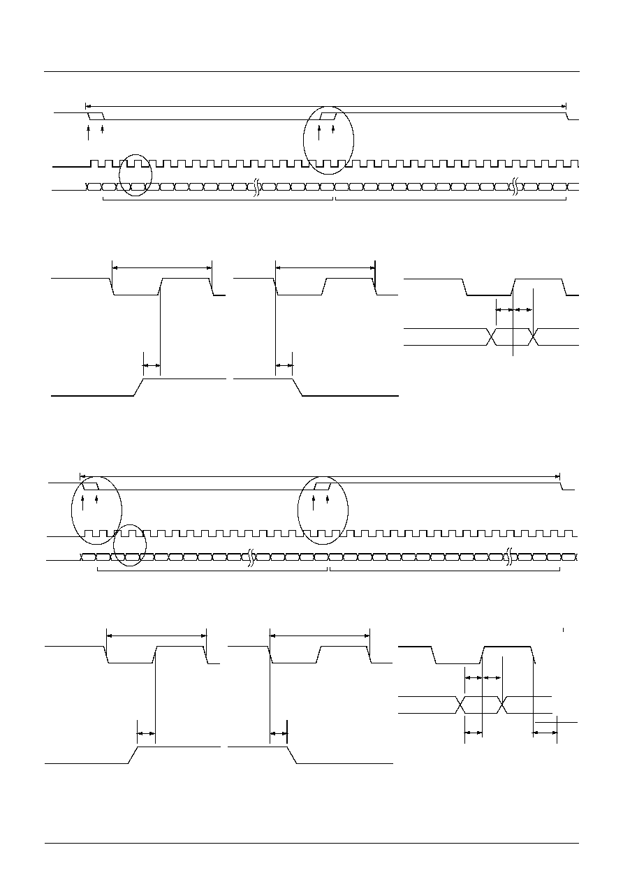
t
s_I2S
I
2
S Input Setup Time
before Rising Edge of Clock
CLI
DAI
10
ns
t
h_I2S
I
2
S Input Hold Time
after Rising Edge of Clock
40
ns
t
d_I2S
I
2
S Output Delay Time
after Falling Edge of Clock
CLI
WSI
30
ns
C
L
=30 pF
t
o_I2S
I
2
S Output Setup Time
before Rising Edge of Clock
CLI
4
ns
C
L
=30 pF
DATA SHEET
UAC 3553B
Micronas
May 21, 2003; 6251-595-1DS
35
Fig. 5�16: Timing: asynchronous I
2
S input
Fig. 5�17: Timing: synchronous I
2
S input
Detail C
WSI as INPUT
1/F
CLI
=325.5 ns
T
s_I2S
CLI - Input
Detail D
WSI as OUTPUT
1/F
CLI
=325.5 ns
T
d_I2S
CLI - Output
R LSB L LSB
16/32 bit right channel
L LSB R MSB
Detail C
PHILIPS format
SONY format
WSI - Input
CLI - Input
DAI - Input
Detail A
PHILIPS format
SONY format
R LSB L MSB
16/32 bit left channel
Detail A
DAI - Input
T
s_I2S
CLI - Input
T
h_I2S
Detail B
WSI as OUTPUT
1/F
CLI
=325.5 ns
T
s_I2S
Detail A
DAI - Input
T
s_I2S
T
o_I2S
T
d_I2S
CLI - Output
CLI - Output
Detail C
WSI as OUTPUT
1/F
CLI
=325.5 ns
T
d_I2S
CLI - Output
R LSB L LSB
16/32 bit right channel
L LSB R MSB
Detail B
PHILIPS format
SONY format
WSI - Input
CLI - Input
DAI - Input
Detail A
PHILIPS format
SONY format
R LSB L MSB
16/32 bit left channel
1/F
I2SWS
Detail C
T
h_I2S
UAC 3553B
DATA SHEET
36
May 21, 2003; 6251-595-1DS
Micronas
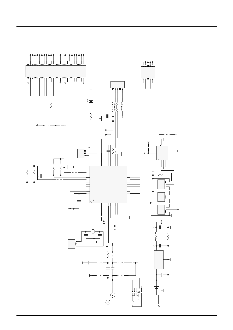
6. UAC 3553B Applications
6.1. Recommended Low-Pass Filters for Analog
Outputs
Fig. 6�1: 2
nd
-order low-pass filter
If the filter is not used, then FOUTL(R), FOPL(R), and
FINL(R) are to be connected (dashed line) and the
internal op-amp must be switched off.
Note: First or third-order low-pass is also possible, but
then the frequency response degrades.
6.2. External Clocking via XTI
AC-coupling of the clock signal
The input level should be in the range of 0.5...2.5 V
PP
.
for a load capacitance of 22 pF at XTO.
DC-coupling of the clock signal
The DC input level must be 0.5
�
V
AREG1
which is typi-
cally 1.75 V. The input level should not exceed
0.5...2.5 V
PP
.
See also Section 2.12. on page 11.
Table 6�1: Attenuation of 2
nd
-order low-pass filter
Frequency
Gain
24 kHz
-
1.5 dB
30 kHz
-
3.0 dB
11 k
220 pF
11 k
11 k
1.0 nF
-
FINL(R)
FOPL(R)
FOUTL(R)
2
nd
-order
AVSS1
D
A
T
A
S
H
E
E
T
U
A
C
3
5
5
3
B
M
i
c
r
o
n
a
s
M
a
y
2
1
,
2
0
0
3
;
6
2
5
1
-
5
9
5
-
1
D
S
3
7
6.3. Typical Applications
Fig. 6�2: Circuit for a typical DAC application
5
N
5
N
5
N
5
N
5
16
5
N
5
N
5
5
5
16
8 $
""AG�@TS
$*1'
Y
!HC
8 "
!!
8 #
!!
$*1'
8$
!!
8 '
#&
$*1'
$*1'
Q$
Svtu�P
Q#
Grs�P
$*1'
$*1'
8!"
$
8!#
$
8 &
!!
$*1'
$9''
8 !
%'
$*1'
8
%'
$*1'
$*1'
8 (
$*1'
8(
$*1'
S"
x
8&
!!
S%
x
S'
x
8
$*1'
S$
x
8'
!!
Q(
'*1'
T8G
T96
!HC
BQDP
BQDP
BQDP!
BQDP"
BQDP#
BQDP$
BQDP%
BQDP&
'9''
'9''
'9''
'9''
*
3
,
2
*
3
,
2
*
3
,
2
*
3
,
2
*
3
,
2
*
3
,
2
*
3
,
2
*
3
,
2
US9`
U@TU
TPA
�S@T
�TVTQ@I9
T@I
T@I
TPA
�TVTQ@I9
�S@T
U@TU
7
5
'
<
6
&
/
6
'
$
QV
VT7�Ur�7
/
)HUULWH
/
)HUULWH
/
)HUULWH
/
)HUULWH
'*1'
'*1'
5
5
&
X9ORZ(65
'*1'
9%86
&
Q
'9''
&
Q
'*1'
&
Q
&(
&(
&(
*
1
'
6'$
6&/
:&
9
&
&
V!
D!8�@@QSPH
'9''
'9''
T8G
'*1'
E%
8@
E#
8@
E!
8@!
'*1'
'9''
XTD
8GD
QD"
D!T�D
'*1'
'$,
:6,
&/,
3.
+HDGSKRQH
9LQ
*
1
'
9RXW
V"
WPGUS@B
9
I#
QPX
&$W�98
'*1'
'*1'
&
X9
&
Q
&
Q
'9''
/
)HUULWH
&
X
9
&
Q
6BI9
6BI9
6W99
.6
vtyr�prpv�v
'/
/('
5
N
9BI9
9W99
9BI9
6'$
&
Q
9BI9
-;
0+]
9%86
'*1'
'9''
0
+
]
'*1'
S!%
x
EQ
T@GA7VT
8"!
!!
S !
!!x
'*1'
'9''
E
8@!
'*1'
�TVTQ@I9
966
9''
7(67
UAC 3553B
5(64
6863(1'4
62)
)
2
8
7
/
)
2
3
/
)
2
8
7
5
)
,
1
/
)
2
3
5
)
,
1
5
1
&
1
&
6
*
1
'
6
5
(
)
1
&
;7,
;72
$5(*
$966
287/
2875
$5(*
$9''
'$,
:6,
&/,
*
3
,
2
*
3
,
2
*
3
,
2
*
3
,
2
*
3
,
2
*
3
,
2
*
3
,
2
6
'
$
*
3
,
2
6
&
/
7
5
'
<
9%86
95(*
'
'
6(1
,&
'$,

All information and data contained in this data sheet are without any
commitment, are not to be considered as an offer for conclusion of a
contract, nor shall they be construed as to create any liability. Any new
issue of this data sheet invalidates previous issues. Product availability
and delivery are exclusively subject to our respective order confirmation
form; the same applies to orders based on development samples deliv-
ered. By this publication, Micronas GmbH does not assume responsibil-
ity for patent infringements or other rights of third parties which may
result from its use.
Further, Micronas GmbH reserves the right to revise this publication and
to make changes to its content, at any time, without obligation to notify
any person or entity of such revisions or changes.
No part of this publication may be reproduced, photocopied, stored on a
retrieval system, or transmitted without the express written consent of
Micronas GmbH.
UAC 3553B
DATA SHEET
38
May 21, 2003; 6251-595-1DS
Micronas
Micronas GmbH
Hans-Bunte-Strasse 19
D-79108 Freiburg (Germany)
P.O. Box 840
D-79008 Freiburg (Germany)
Tel. +49-761-517-0
Fax +49-761-517-2174
E-mail: docservice@micronas.com
Internet: www.micronas.com
Printed in Germany
Order No. 6251-595-1DS
7. Data Sheet History
1. Final data sheet: "UAC 3553B Universal Serial Bus
(USB) DAC", Edition May 21, 2003, 6251-595-1DS.
First release of the final data sheet.